Electron Microscopy Sciences Lattice Scriber for Semiconductor Wafers
Shop Electron Microscopy Sciences Lattice Scriber for Semiconductor Wafers at
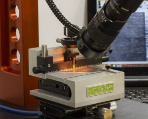
LatticeGear – New Dimensions in Scribing and Cleaving
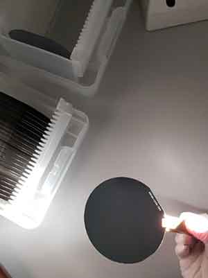
What are Silicon Wafers used for?

Nano−Micro Characterization of Defects on Silicon Surfaces: An

Sliding History-Dependent Adhesion of Nanoscale Silicon Contacts

BMD densities and sizes determined by optical microscopy

PDF] Design of the Transmission Electron Microscope (TEM) Sample
Electron Microscopy Sciences: Microscopy Lab Supplies

Electron Microscopy Sciences Wafer Cleaving Station

Sample Preparation for Semiconductor Devices: A Complete Picture
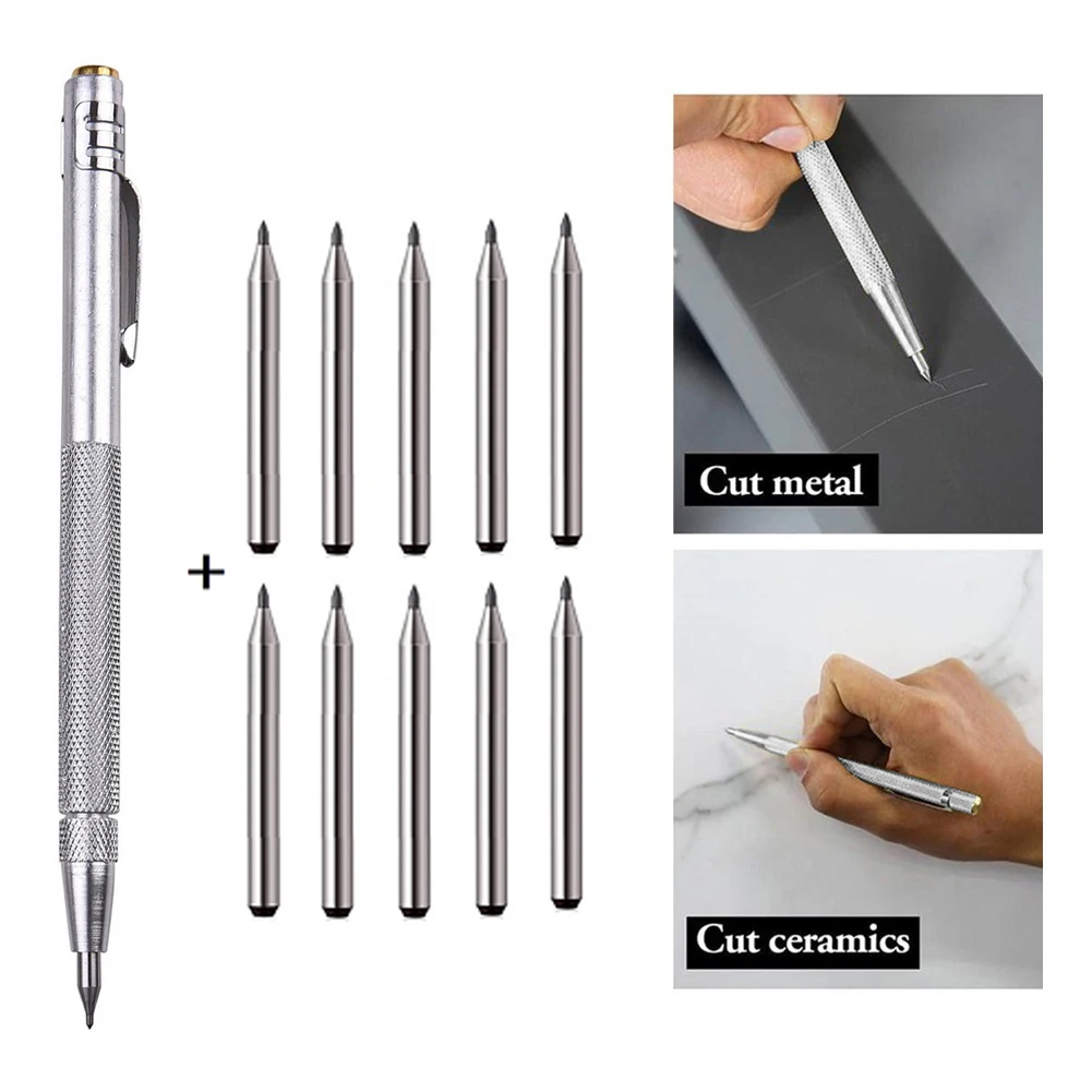
This is the best scriber you'll ever find for scribing semiconductor wafers. This custom scriber has an eight point truncated diamond tip that can be

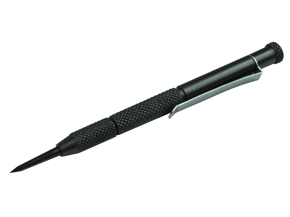
Lattice Scriber

Volume scanning electron microscopy for imaging biological