silk screen technique for homemade pcb - General Electronics - Arduino Forum
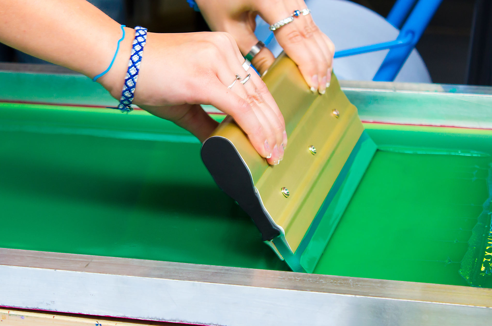
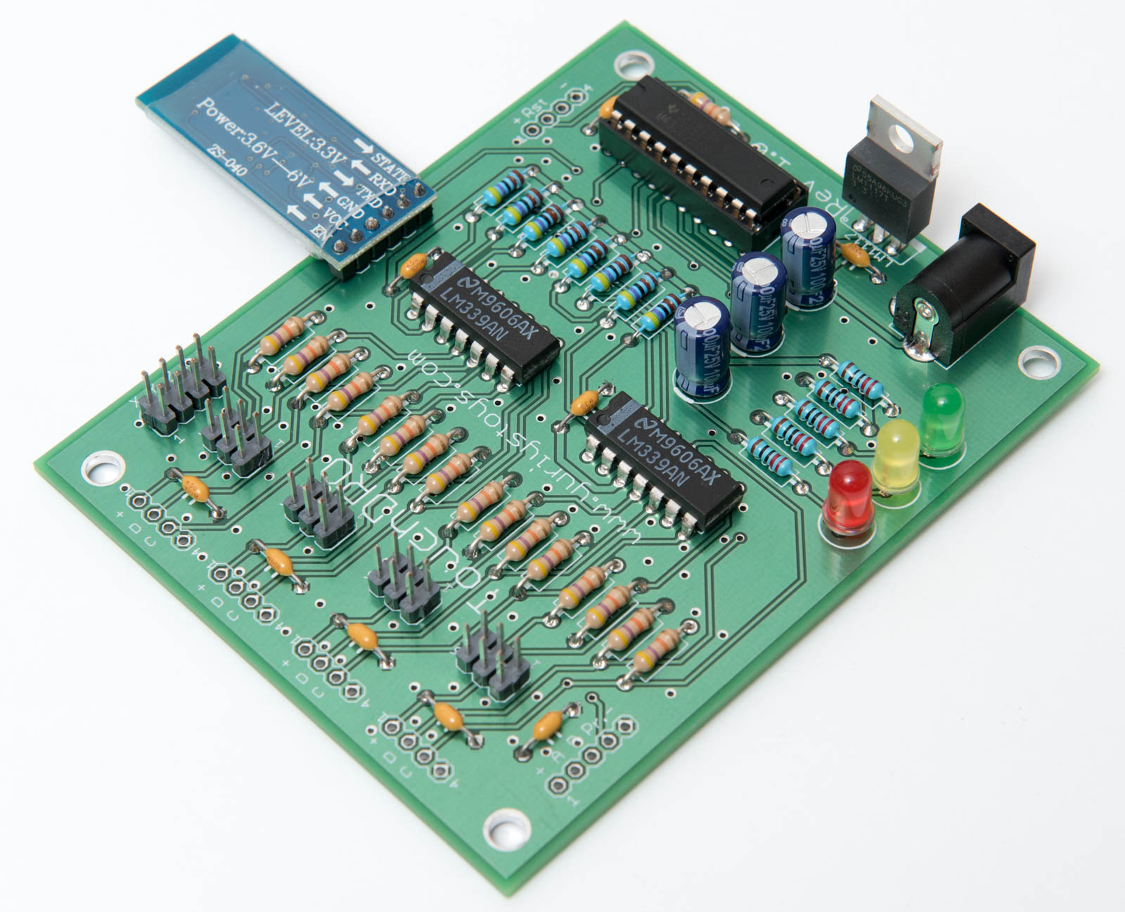
I've been working on getting a nice homemade silkscreen technique for my PCBs. I have never had good results with toner transfer. I would like to know what you think of my latest efforts and if I should move forward with this. Please note, this is a first attempt and not all of the holes/components line up with the silk screen. I just wanted to see if I could do it.

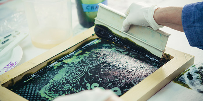
DIY PCB silkscreen cheap, easy and fast

Simple Design Techniques that could Reduce your PCB Manufacturing Cost
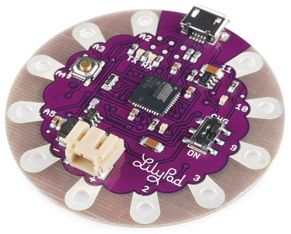
PCB Basics - SparkFun Learn

Silk screening vs toner transfer PCB - General Electronics - Arduino Forum

New Tutorial! PCB Silkscreen Layers in @adskeagle video by @ecken « Adafruit Industries – Makers, hackers, artists, designers and engineers!

DIY Pico GPIO Expansion Board – Project Corner – DroneBot Workshop Forums
Arduino.org, Page 12
Top ten tips for nailing your PCB silkscreen design
How to Build the Mixed Scale Digital Readout Kit

Another OPP Carrier Board for MPF use

Working on a Minidexed modular conversion - DIY STUFF - Look Mum No Computer Thingies

Highly Liquid Projects - Page 2 - MOD WIGGLER